The global artificial intelligence hardware sector is witnessing a pivotal transformation as NVIDIA formally qualifies HBM4 samples from the three dominant memory manufacturers. This milestone officially confirmed through recent announcements, executive statements, and supply chain movements signals the beginning of a new computational era. The qualification of fourth-generation High Bandwidth Memory (HBM4) samples by NVIDIA is not merely a routine supplier evaluation; it represents the final breaking of the “Memory Wall” that has constrained AI performance for nearly a decade .
For the first time in the history of accelerator design, memory is no longer a passive storage component. With NVIDIA’s qualification of 12-layer and 16-layer HBM4 stacks from SK Hynix, Samsung Electronics, and Micron Technology, the industry has officially entered an age where memory stacks contain active logic dies manufactured on advanced foundry nodes. This architectural evolution enables bandwidth exceeding 3.3 TB per second, per-pin speeds surpassing 11 Gbps, and single-GPU memory capacities approaching half a terabyte .
This comprehensive analysis examines the technical breakthroughs driving NVIDIA’s HBM4 qualification, the competitive dynamics among the three memory juggernauts, the strategic implications for the Rubin and Vera Rubin platforms, and the broader consequences for the trillion-parameter AI models that will define the remainder of this decade.
Understanding the NVIDIA HBM4 Qualification: Definition and Significance
Before dissecting the competitive landscape, it is essential to understand what NVIDIA’s “qualification” of HBM4 samples actually entails. In the semiconductor industry, qualification is the rigorous, multi-stage validation process through which a chip designer verifies that a supplier’s memory components meet specific performance, reliability, power, and thermal requirements under real-world operating conditions.
NVIDIA’s HBM4 qualification process is widely regarded as the most stringent in the industry. Unlike JEDEC standard compliance, which provides a baseline for interoperability, NVIDIA imposes custom specifications that far exceed official standards. According to industry reports, NVIDIA has mandated per-pin data rates exceeding 11 Gbps, with specific configurations targeting 13 Gbps a significant increase from the JEDEC range of 6.4 Gbps to 9.6 Gbps .
The qualification process involves multiple phases:
-
A. Initial Sample Validation: Memory vendors submit engineering samples to NVIDIA for preliminary electrical and functional testing. This phase identifies fundamental defects in circuit design, signal integrity, and power delivery. SK Hynix began this Customer Sample certification process in October 2025 .
-
B. System-in-Package Integration Testing: HBM4 stacks are integrated with NVIDIA’s Rubin GPU prototypes using TSMC’s CoWoS-L advanced packaging technology. This phase evaluates how the memory interacts with the compute die under high-bandwidth conditions, including thermal management and power distribution network stability .
-
C. Environmental and Stress Qualification: Memory samples undergo rigorous testing under extreme temperature, humidity, voltage, and mechanical stress conditions. Reports indicate that NVIDIA’s environmental testing requires HBM4 to maintain 9–10 Gbps performance under these harsh conditions a demanding criterion that has delayed several suppliers .
-
D. Volume Production Readiness Certification: Once engineering samples pass all technical evaluations, NVIDIA audits the supplier’s manufacturing yield, capacity, and quality control systems. This final stage determines whether the supplier can deliver consistent, high-volume shipments to support NVIDIA’s production schedules .
The successful qualification of HBM4 samples by all three memory manufacturers confirmed through various official channels in January and February 2026 represents a collective triumph of advanced packaging, circuit design, and process engineering. However, the path to this achievement has been fraught with technical setbacks, redesign mandates, and intense competitive maneuvering.
The Technical Revolution Inside HBM4: Why Qualification Was So Difficult
To appreciate the magnitude of NVIDIA’s HBM4 qualification achievement, one must understand the unprecedented technical complexity embedded within these fourth-generation memory stacks. HBM4 is not merely an incremental improvement over HBM3e; it is a fundamental re-architecture of how memory is built, integrated, and utilized.
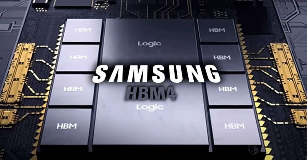
The 2048-Bit Interface and the Doubling of Bandwidth
The most significant architectural change in HBM4 is the expansion of the interface width from 1024 bits to 2048 bits. This doubling of the data “pipe” enables aggregate bandwidth exceeding 2.0 TB per second per stack in initial implementations, with Samsung achieving 3.3 TB per second in its qualified 12-layer samples .
This wider interface, however, presents severe physical design challenges. Doubling the number of input/output pins within the same physical footprint requires extreme miniaturization of through-silicon vias and micro-bumps. Memory manufacturers have had to develop new signaling technologies to manage power consumption and signal integrity across this dense interconnect fabric. Samsung addressed this by implementing low-voltage design techniques for data transmission through TSVs and optimizing the power distribution network, achieving 40% improvement in energy efficiency compared to the previous generation .
The Active Logic Die: Memory Becomes a Processor
Perhaps the most transformative aspect of HBM4 is the integration of a logic die at the base of the memory stack. For the first time, the interface die is being manufactured on advanced foundry processes 12nm, 5nm, and 4nm nodes rather than legacy DRAM processes. This enables the memory stack to perform active processing functions, including data pre-processing, compression, and even basic neural network operations .
This architectural shift has profound implications. By offloading certain data manipulation tasks to the memory stack itself, HBM4 reduces round-trip latency to the GPU and lowers the bandwidth burden on the main compute die. Industry analysts estimate that this active memory capability improves overall system energy efficiency by approximately 30% while simultaneously reducing the heat generation that plagued early high-stack HBM3e implementations .
The Stacking Challenge: From 12-Hi to 16-Hi
NVIDIA’s qualification process has simultaneously validated both 12-layer (12-Hi) and 16-layer (16-Hi) HBM4 stacks. The 16-Hi configuration is particularly significant because it pushes the physical limits of DRAM stacking to unprecedented extremes.
To fit 16 DRAM layers within the JEDEC-mandated package height of 775 micrometers, memory manufacturers must thin each wafer to approximately 30 micrometers roughly one-third the thickness of a human hair. This extreme thinning creates severe challenges with wafer warpage, structural integrity, and thermal dissipation .
Different manufacturers have adopted distinct approaches to overcoming this challenge:
-
SK Hynix continues to refine its Advanced Mass Reflow Molded Underfill (MR-MUF) process, which simultaneously interconnects all stacked chips in a single thermal compression step. The company introduced new Epoxy Molding Compound materials that improve heat dissipation by 1.6 times compared to previous generations .
-
Samsung is aggressively pursuing copper-to-copper hybrid bonding technology, which eliminates micro-bumps entirely by directly fusing copper pads between layers. While this approach promises superior electrical performance and thinner stacks, current yields remain low approximately 10% for hybrid-bonded prototypes .
-
Micron has focused on optimizing its thermal compression with non-conductive film (TC-NCF) process while rapidly expanding capacity through new facilities in Singapore and Hiroshima .
The Pin Speed War: Exceeding 11 Gbps
NVIDIA’s aggressive specification scaling has been the primary driver of technical difficulty in HBM4 qualification. The company’s requirement for per-pin speeds exceeding 11 Gbps with targets as high as 13 Gbps has forced multiple redesign cycles across the supply chain .
Samsung achieved pin speeds of 11.7 Gbps in its qualified HBM4 samples, representing a 46% increase over the baseline JEDEC standard of 8 Gbps. The company states that its architecture is scalable to the maximum 13 Gbps target, positioning it favorably for higher-end Rubin configurations . SK Hynix has similarly demonstrated 11.7 Gbps performance in its 16-Hi demonstrations, while Micron has confirmed speeds exceeding 11 Gbps in its production-qualified parts .
The Tri-Polar Competition: How Each Vendor Won NVIDIA Qualification
The successful qualification of HBM4 samples by all three memory manufacturers masks a fierce, multi-dimensional competitive battle. Each vendor has pursued distinct technological strategies, manufacturing philosophies, and supply chain partnerships to secure their position in NVIDIA’s ecosystem.
A. SK Hynix: The Incumbent Champion Leveraging the “One Team” Strategy
SK Hynix entered the HBM4 qualification race as the undisputed market leader, having dominated HBM3 and HBM3e supply to NVIDIA. The company’s strategy centers on deepening its strategic alliance with Taiwan Semiconductor Manufacturing Company (TSMC).
By outsourcing the critical logic base die to TSMC’s 5nm and 12nm foundry nodes, SK Hynix ensures seamless integration with NVIDIA’s CoWoS-L packaging flow. This “One Team” approach creates a formidable technical and commercial barrier: because SK Hynix’s memory is explicitly tuned for TSMC’s interposer technologies, it offers NVIDIA lower integration risk and faster time-to-market .
SK Hynix achieved “meaningful results” in NVIDIA’s System-in-Package tests during January 2026, successfully addressing earlier circuit defects through design modifications and process adjustments. The company demonstrated 9–10 Gbps performance under NVIDIA’s stringent environmental testing conditions, confirming the robustness of its MR-MUF packaging technology .
Perhaps most significantly, SK Hynix became the first manufacturer to publicly demonstrate 16-layer HBM4 at CES 2026. This 48 GB stack establishes an early leadership position in the high-capacity segment that will be essential for Rubin Ultra configurations and the eventual transition to 100-trillion parameter models .
B. Samsung Electronics: The Vertical Integration Challenger
Samsung’s qualification represents a remarkable turnaround. After lagging in HBM3e, the company has executed an aggressive catch-up strategy centered on its unique “turnkey” capability the ability to manufacture both the DRAM core dies and the logic base die internally.
Samsung’s qualified HBM4 samples incorporate two distinctive technological advantages:
First, Samsung is the only vendor applying 1c DRAM process technology (10-nanometer class, sixth generation) to its HBM4 stacks. Competitors initially built HBM4 on the older 1b node, forcing later redesigns when NVIDIA raised performance requirements. Samsung’s early adoption of 1c DRAM, with yields reportedly approaching the 80% mass-production target, provided critical headroom for speed scaling .
Second, Samsung leverages its in-house 4nm foundry capability for the logic base die. This vertical integration allows Samsung to optimize the interface between DRAM and logic without the coordination overhead of cross-company partnerships. Executive Vice President Hwang Sangjoon emphasized that this approach enabled Samsung to “secure sufficient headroom for performance scaling through process competitiveness and design improvements” .
The company formalized its qualification achievement through an unprecedented announcement on February 12, 2026, confirming first mass production and shipment of HBM4 to NVIDIA. President and CTO Song Jae-hyuk described customer feedback as “very satisfactory,” signaling that Samsung has successfully met NVIDIA’s elevated specifications .
C. Micron Technology: The Efficiency Specialist Overcoming Exclusion Rumors
Micron’s path to HBM4 qualification has been the most turbulent. In early February 2026, semiconductor supply chain analyst firm Semianalysis published a report claiming that Micron had been entirely excluded from NVIDIA’s HBM4 supplier list for the flagship VR200 NVL72 system, with SK Hynix securing 70% allocation and Samsung capturing the remaining 30% .
The report attributed Micron’s alleged exclusion to NVIDIA’s “aggressive memory specification scaling” the increase from 13 TB/s bandwidth targets in March 2025 to the final 22 TB/s specification confirmed at CES 2026, representing a nearly 70% increase in performance requirements .
However, Micron Chief Financial Officer Mark Murphy delivered a forceful public rebuttal at the Wolfe Research Presentation on February 11, 2026. Murphy explicitly confirmed that Micron’s HBM4 has “passed NVIDIA certification,” has “already begun shipping,” and has entered “high-volume production.” He further disclosed specific product specifications: 36GB capacity and speeds exceeding 11 GB/s (likely a reference to gigabits per second) .
Murphy’s statement that Micron’s 2026 HBM supply capacity is “100% sold out” suggests that while the company may face allocation constraints relative to its Korean rivals, it has successfully secured a position in NVIDIA’s supply chain .
Industry observers note that the “truth” likely resides in market realities. With HBM4 supply severely constrained and NVIDIA facing insatiable demand, the company has strong incentives to qualify multiple sources. As long as Micron’s technical specifications cross NVIDIA’s minimum thresholds, maintaining a diversified supply base reduces risk and increases negotiating leverage .
Furthermore, Micron has secured a strategic foothold through an alternative pathway: supplying LPDDR5X memory for NVIDIA’s Vera CPU. The Vera processor, built around NVIDIA’s custom “Olympus” Arm cores, utilizes SOCAMM2-specification LPDDR5X modules. In this specific memory segment, Micron is considered the largest potentially exclusive supplier, with single CPU configurations supporting up to 1.5 TB of LPDDR5X memory .
The Rubin and Vera Rubin Platforms: Why HBM4 Qualification Matters
The qualification of HBM4 samples is not an abstract technological achievement; it is the critical enabler for NVIDIA’s next-generation AI platforms. Understanding the qualification’s significance requires examining the systems these memory components will power.
The Rubin GPU Architecture
The Rubin GPU, named after astronomer Vera Rubin, represents a fundamental departure from NVIDIA’s previous architectural approaches. Manufactured on TSMC’s 3nm-class process technology, Rubin utilizes a sophisticated multi-die chiplet design featuring two reticle-limited compute dies .
This architecture delivers unprecedented computational density: 50 petaflops of FP4 performance in the base configuration, doubling to 100 petaflops in the Rubin Ultra variant. To sustain this computational throughput, the memory subsystem must deliver commensurate bandwidth and capacity requirements that only HBM4 can satisfy .
NVIDIA’s qualified HBM4 samples enable Rubin configurations with 8 to 12 memory stacks, each providing between 24 GB and 48 GB of capacity. This yields total VRAM configurations ranging from 288 GB to 576 GB per GPU a 4x to 8x increase over current-generation HBM3e systems .
The Vera CPU Integration
The Rubin platform introduces another critical component: the Vera CPU, NVIDIA’s first fully custom, Arm-compatible processor built around the “Olympus” core architecture. Vera communicates with the Rubin GPU through NVLink-Chip-to-Chip (NVLink-C2C) interconnects operating at 1.8 TB/s .
This CPU-GPU coherence places extraordinary demands on the HBM4 subsystem. The memory must simultaneously service GPU compute threads and maintain coherency with the CPU’s memory space across the high-speed interconnect. NVIDIA’s elevated pin-speed requirements exceeding 11 Gbps are directly driven by this unified memory architecture .
The VR200 NVL72 Rack Solution
The most demanding application for qualified HBM4 is the VR200 NVL72 rack-scale solution, scheduled for shipment in late summer 2026. This system integrates 72 Rubin GPUs and 72 Vera CPUs into a single, liquid-cooled rack with 22 TB/s of aggregate bandwidth .
Achieving this bandwidth requires not only high per-pin speeds but also precise matching of electrical characteristics across thousands of HBM4 stacks. This explains why NVIDIA’s qualification process has been so exhaustive and why the simultaneous qualification of three suppliers represents such a significant achievement.
Timeline of Qualification: From Redesign to Mass Production
The path to HBM4 qualification has been marked by shifting timelines, redesign mandates, and intense speculation. Understanding this chronology illuminates both the technical challenges and the competitive dynamics among memory suppliers.
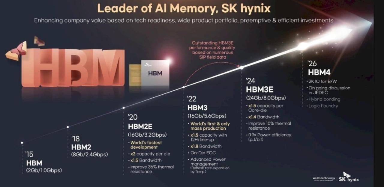
September 2025: SK Hynix establishes mass production system for HBM4, becoming the first vendor to reach this milestone .
October 2025: SK Hynix begins Customer Sample certification process with NVIDIA. Initial testing reveals circuit defects requiring design modifications .
November-December 2025: NVIDIA raises HBM4 pin-speed requirements, mandating speeds exceeding 11 Gbps. This triggers redesigns across all three memory manufacturers. Initial mass production timeline for Rubin platform pushed to late Q1 2026 .
December 2025: Samsung and SK Hynix begin delivering paid final HBM4 samples to NVIDIA .
January 8, 2026: TrendForce reports that NVIDIA’s elevated requirements have forced all three memory makers to resubmit HBM4 samples .
January 9, 2026: SK Hynix demonstrates 16-layer HBM4 at CES 2026, showcasing 48 GB capacity and 11.7 Gbps speeds .
January 29, 2026: SK Hynix achieves “meaningful results” in NVIDIA’s HBM4 System-in-Package tests. Optimized products meet 11 Gbps target bandwidth and maintain 9–10 Gbps under environmental stress conditions .
January 30, 2026: SK Hynix confirms in earnings call that HBM4 development is “proceeding as scheduled” with mass production of customer-requested volumes already underway .
February 9, 2026: Semianalysis report claims Micron excluded from HBM4 supply for VR200 NVL72, with SK Hynix securing 70% and Samsung 30% allocation .
February 11, 2026: Micron CFO Mark Murphy publicly refutes exclusion claims, confirming HBM4 has passed NVIDIA certification and shipments have commenced .
February 12, 2026: Samsung formalizes first mass production and shipment of HBM4, announcing 11.7 Gbps speeds, 3.3 TB/s bandwidth, and 40% energy efficiency improvement .
February 2026: SK Hynix plans to begin large-scale HBM4 shipments .
Late Q1 2026: Expected start of full-volume HBM4 mass production across all three suppliers .
Economic and Geopolitical Implications
The successful qualification of HBM4 samples by three suppliers carries implications far beyond technical specifications. This milestone reshapes the economics of the AI industry and exposes underlying geopolitical vulnerabilities.
The Cost Escalation Trap
HBM4 is dramatically more expensive than any preceding memory generation. Industry sources indicate that HBM4 costs five to seven times more than standard DDR5 memory on a per-gigabyte basis . This cost escalation is driven by several factors:
-
The need for advanced foundry nodes (4nm, 5nm, 12nm) for logic base dies
-
Extremely low yields during early production phases
-
The complexity of 16-layer stacking with 30-micrometer wafer thinning
-
Limited manufacturing capacity concentrated in three companies
This cost structure threatens to widen the “Silicon Divide” between hyperscale cloud providers and smaller AI startups. Microsoft, Meta, Google, and Amazon can absorb HBM4 costs through massive volume commitments and internal AI service monetization. Independent AI companies face the prospect of paying significantly more for computing capacity, potentially accelerating industry consolidation .
Supply Chain Concentration Risk
The HBM4 qualification milestone also exposes extreme geographic concentration in the AI supply chain. 100% of HBM4 production is concentrated in South Korea (SK Hynix, Samsung) and the United States (Micron) , with critical logic base die manufacturing dependent on TSMC in Taiwan .
This concentration creates strategic vulnerabilities. Any disruption whether from geopolitical conflict, natural disaster, or pandemic could paralyze the global AI industry. NVIDIA has attempted to mitigate this risk by qualifying multiple suppliers, but all three remain dependent on TSMC’s advanced packaging capacity for final CoWoS-L integration .
The NVIDIA Supplier Lock-In Effect
Perhaps the most significant economic implication is the reinforcement of NVIDIA’s position as the “gravity well” of the AI industry. By setting specifications that exceed JEDEC standards and forcing memory makers into multi-billion-dollar investments in unproven technologies, NVIDIA effectively dictates the roadmap for the entire semiconductor ecosystem .
CEO Jensen Huang explicitly acknowledged NVIDIA’s unique position, noting that the company will be the “initial exclusive user of HBM4 for quite a long time” . This exclusivity gives NVIDIA unprecedented leverage over both suppliers and customers. Memory manufacturers must align their development schedules with NVIDIA’s roadmap; cloud providers must secure server manufacturing capacity years in advance; AI startups must optimize their models for NVIDIA’s specific memory configurations.
Future Roadmap: Beyond HBM4 Qualification
The successful qualification of initial HBM4 samples represents not an终点 but a starting point. The memory industry is already racing toward the next generation of products and technologies.
HBM4E and the 16-Layer Transition
While 12-layer HBM4 has only recently entered mass production, NVIDIA has already requested 16-layer HBM4 supply for the second half of 2026 . This accelerated timeline reflects the insatiable demand for memory capacity driven by trillion-parameter models.
The transition to 16 layers presents formidable technical challenges. SK Hynix has demonstrated early 16-Hi samples using advanced MR-MUF, while Samsung is racing to improve yields on its hybrid bonding prototypes. The company that successfully masters high-volume 16-layer production will capture the majority of NVIDIA’s high-end Rubin Ultra orders .
Hybrid Bonding: The Make-or-Break Technology
Industry consensus holds that hybrid bonding is essential for HBM5 and beyond. As layer counts increase beyond 16, the cumulative thickness of micro-bumps becomes prohibitive. Direct copper-to-copper bonding eliminates these bumps entirely, enabling thinner stacks and improved thermal performance .
Samsung currently leads in hybrid bonding development, having already supplied prototypes to NVIDIA. However, yields remain distressingly low approximately 10% suggesting that volume production remains years away. SK Hynix is developing hybrid bonding as a “fallback” technology while extending MR-MUF as far as possible .
Custom HBM and the Logic Die Revolution
The integration of foundry-process logic dies at the base of HBM4 stacks opens a fascinating possibility: custom HBM tailored to specific AI workloads. Future generations may see AI labs like OpenAI, Anthropic, or Google designing their own logic dies, optimized for their unique neural network architectures .
This would represent the ultimate convergence of memory and processing, transforming HBM from a standardized commodity into a customizable AI accelerator component. NVIDIA’s qualification of initial HBM4 samples has opened this door; it remains to be seen who will walk through it.
Conclusion: The Memory Wall Has Fallen

The qualification of HBM4 samples from SK Hynix, Samsung Electronics, and Micron Technology marks a decisive turning point in the history of artificial intelligence hardware. For years, the “Memory Wall” the growing disparity between processor speed and memory bandwidth threatened to halt AI scaling. Each generation of neural networks demanded more data than the previous generation’s memory systems could supply.
With HBM4, that wall has been breached. Three terabytes per second per stack. Eleven gigabits per second per pin. Five hundred twelve gigabytes per GPU. Forty percent improvement in energy efficiency.
These are not incremental advances. They are architectural revolutions enabled by the transformation of memory from passive storage to active logic. The base die of an HBM4 stack, manufactured on 4nm or 5nm foundry processes, contains more computational capability than entire servers from a decade ago. This is no longer merely memory; it is computation embedded within memory.
The competitive battle among the three qualified suppliers is far from over. SK Hynix leads in early 16-layer demonstrations and maintains the closest integration with TSMC’s packaging ecosystem. Samsung has executed a remarkable turnaround through vertical integration and aggressive 1c DRAM adoption. Micron has weathered speculation about its exclusion to secure certification and establish a complementary position in Vera CPU memory.
Yet the ultimate victor is NVIDIA. By qualifying three suppliers simultaneously, NVIDIA has secured the diversified, high-volume supply chain necessary to ship millions of Rubin GPUs. By setting specifications that exceed industry standards, NVIDIA has forced the entire memory industry to align with its architectural vision. By locking in server manufacturing capacity through 2026, NVIDIA has ensured that it and it alone controls the flow of the world’s most valuable commodity: AI compute capacity.
The HBM4 qualification milestone is therefore both an ending and a beginning. It concludes the era of memory as a commodity bottleneck and inaugurates the era of memory as a strategic weapon. The companies that master HBM4 and its successors will not merely supply components; they will define the physical infrastructure upon which artificial general intelligence will be built.


